

 English
 中文
中文
Call Us Now
TEL: +86 13386078659; Skype ID: Hanwei; WeChat: +8613386078659; QQ ID: 413882258.

Item No.:
TR-IONINPayment:
EXW, FOB, CIF.Product origin:
ChinaColor:
Shipping port:
ShangHaiLead Time:
60
TEL: +86 13386078659; Skype ID: Hanwei; WeChat: +8613386078659; QQ ID: 413882258.
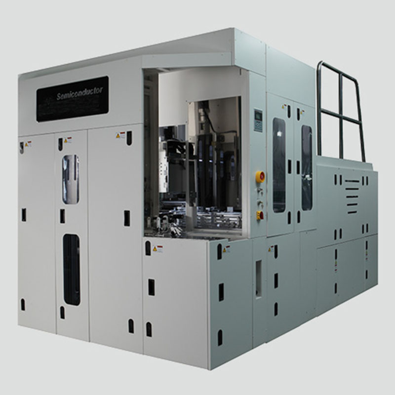
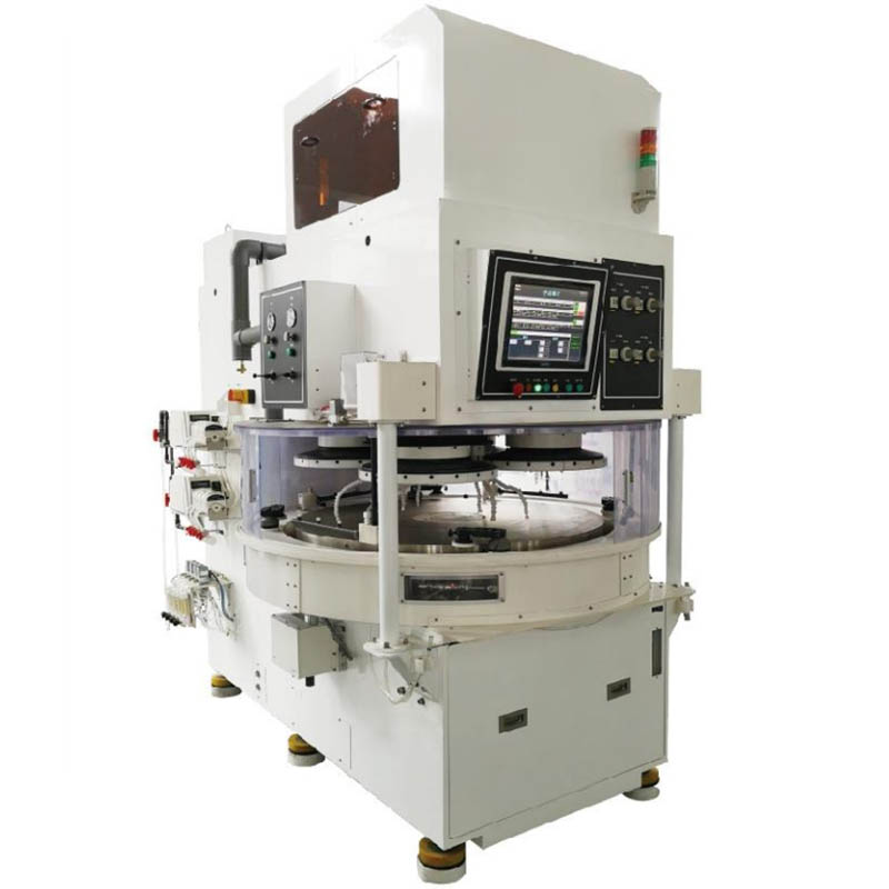
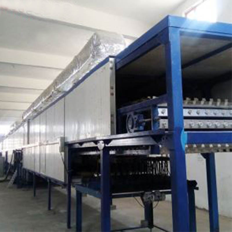
Ion Implantation:
Ion implantation is a process that changes its characteristics by doping a certain element on the surface of a semiconductor material, and is widely used in the integrated circuit (IC) industry. As the equipment of the ion implantation process, the ion implanter is one of the most critical tools in the advanced IC production line, with a global market size of 1.5-2 billion US dollars every year.
Compared with the doping technology of thermal diffusion, the ion implantation technology has the following characteristics: single-sided collimated doping, good doping uniformity and controllability, the singleness of doping elements, and it is easy to realize the doping area. Graphical.
These features bring advantages that thermal diffusion does not have in the manufacture of crystalline silicon solar cells—not only can high-quality PN junctions be formed, the conversion efficiency of cells can be improved, but also the manufacturing process of various high-efficiency cells can be greatly simplified: conventional cells The production of phosphosilicate glass and edge etching can be eliminated; the production of double-sided cells can eliminate the masking process; in addition, the zonal doping necessary for back-contact cells can eliminate the alignment process, which greatly reduces the The manufacturing cost of such batteries is reduced. Ion implantation is an economical and reliable technique for improving cell efficiency and making high-efficiency cells.
In addition, since toxic emission processes such as phosphorus/boron diffusion, dephosphorization/borosilicate glass, and edge etching are omitted, ion implantation can significantly reduce environmental pollution caused by cell production.
However, the low productivity, high cost and huge footprint of IC ion implanters make the ion implantation technology not yet widely used in the photovoltaic industry. According to the actual situation and needs of solar cell technology, Shanghai Keystone Semiconductor Co., Ltd. has customized a large-beam ion implanter-IonSolar for the photovoltaic industry. In the transmission and ion beam current system of silicon wafers, IonSolar has applied a number of major breakthrough technologies with independent intellectual property rights: the "curtain" wide-width ion beam of a single implanted element can be "shower" without interruption to the uniform transmission. On monocrystalline silicon wafers, stable and uniform element doping is achieved, and high productivity and low manufacturing costs are ensured, providing an effective way for the production line upgrade of solar cells and the production of high-efficiency cells.
• Small footprint
IonSolar covers an area of 22m2 and realizes technological upgrading without changing the layout of the existing production line.
• Low process cost
The process cost of IonSolar is only 60% of that of similar products, with low investment and short payback period.
• Local manufacturing and service
European and American quality standards, localized services, fast and efficient.
Founded by a team of well-known overseas experts with experience in successfully developing multiple generations of IC ion implanters. We have realized the localization of high-quality and high-performance ion implanters; we have taken an important step in the road of "Made in China" and "Created in China!"
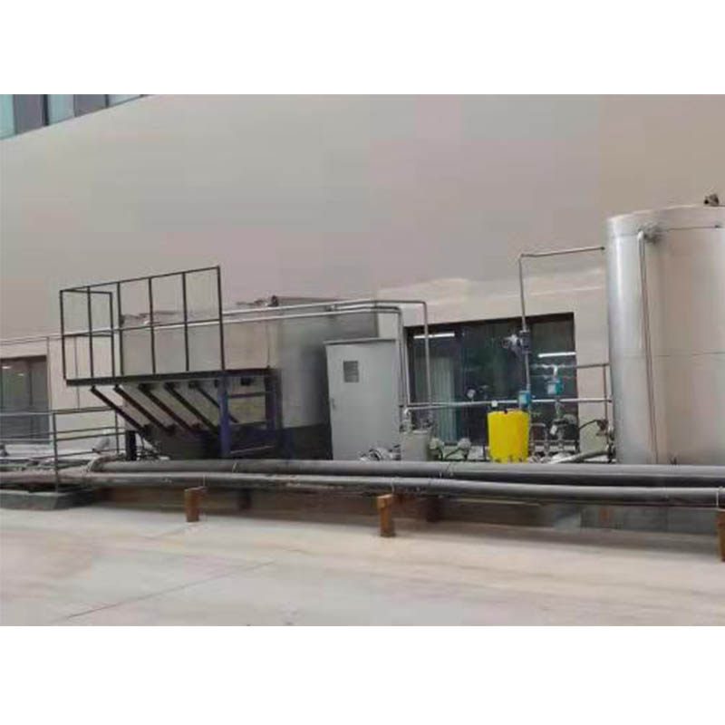
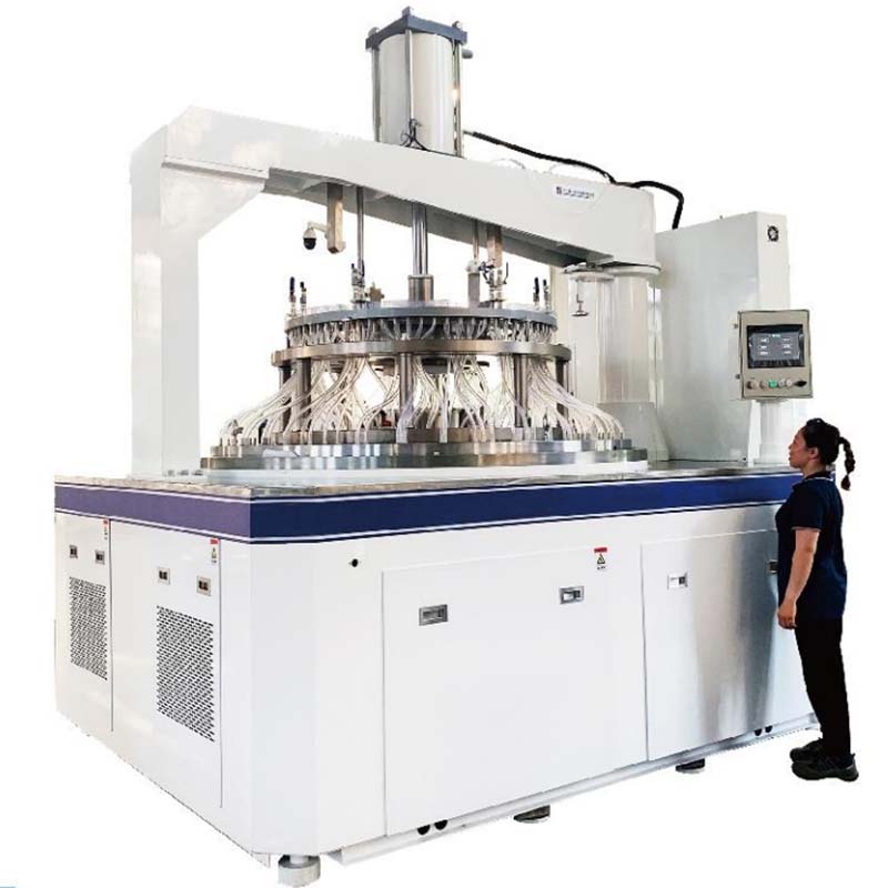
Wastewater Treatment Equipment Ranges: 1. Removal of suspended solids in wastewater after biochemical treatment. 2. Solid-l
Ion implantation equipment Features: • high productivity IonSolar has the function of continuous film feeding, and the produ
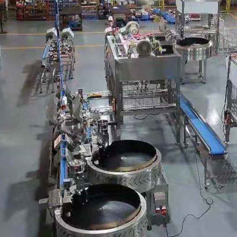
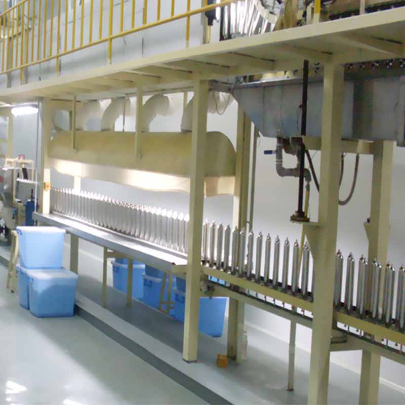
Automatic glove dipping line features: This machine by PLC program control with automatic and manual modes, its simple operation, small size, and use gloves Rol...
Single side grinding/polishing machine: Name: Single-sided copper plate polishing machine TR-ES50B Machine size: Length 2450㎜×Width 1721㎜×Height 2900㎜ Machi...
Wafer Polishing Machine High-precision double-sided grinding polishing machine TR-32B Mechanical Dimensions: Length 3850㎜×Width 2900㎜×Height 3700㎜ Machine we...
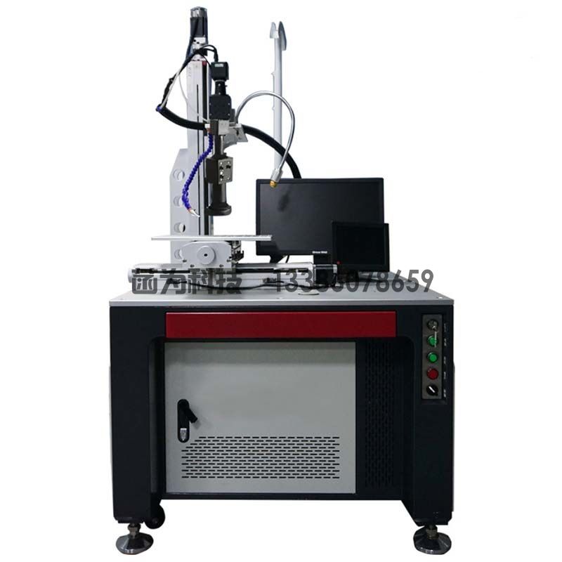
Equipment Principle: The galvanometer laser welding machine is a perfect combination of the galvanometer motion system and t
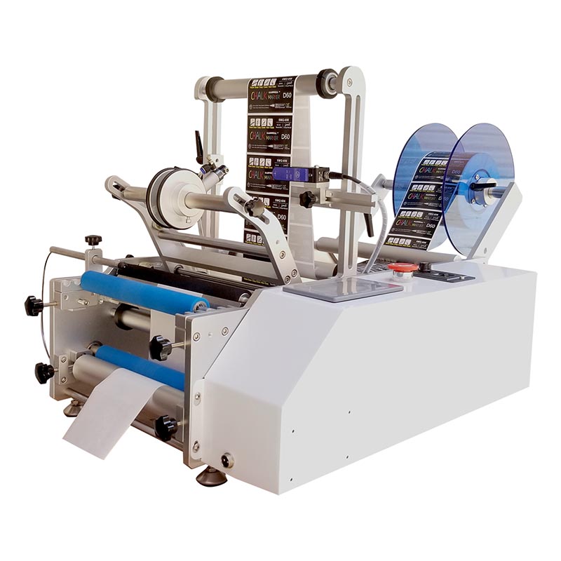
Semi auto labeling machine applications:It can be used for labeling various specifications of cylindrical objects, such as re
A professional design, manufacture all kinds of gloves equipment production enterprise, its excellent product quality and fir
This equipment is a high-quality product developed by ourselves according to market demand after learning the advantages of E
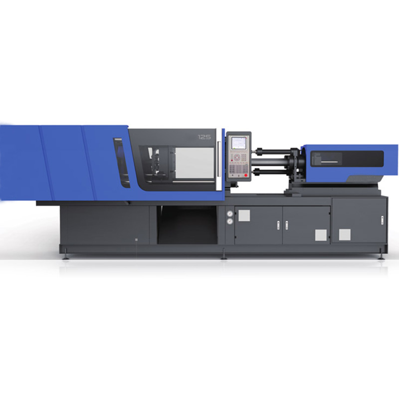
TR series servo energy-saving injection molding machines: Precise clamping system, outstanding efficiency, efficient servo dr
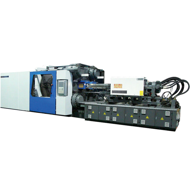
Injection molding machine equipment:Precise locking system, outstanding efficiency, efficient servo drive, all meet all requi
Equipment Fetures: * High Speed process up to 600pcs/min. * Large payload of Delta Robot by 7kg. * Japanese Panasonic Servo M
Ourmanufacturer‘s research and development, design and produce machines of gloves,balloon and condom. Mainly in balloon print
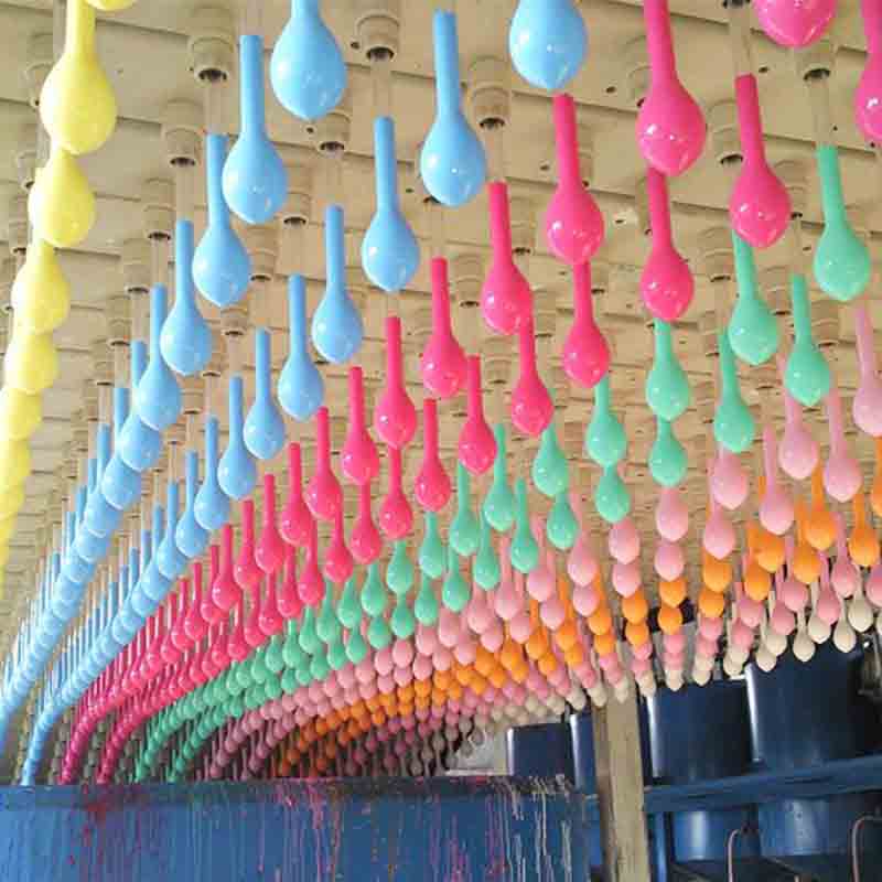
The system of latex balloon dipping machine realized communication controlled by humanity-machine interface. They raise the d
1.It adopts the newest type high-power transmission mechanism to arrange the chain and drive the main driving shaft. The erro
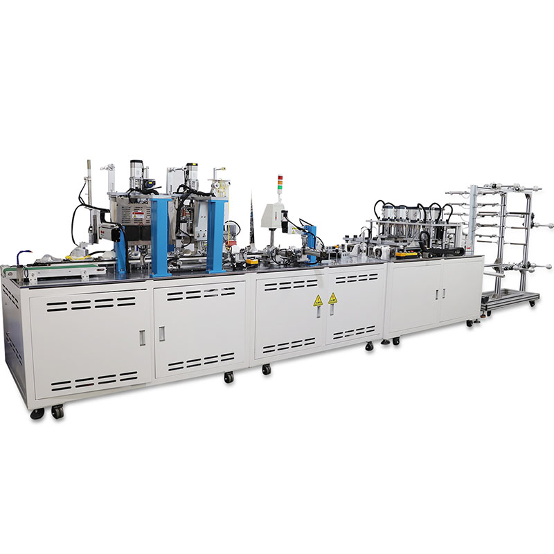
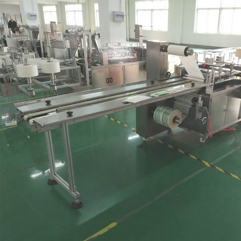
Production Model: Cup type Speed: 25+pc/min Rate of defect prodcution: Less than 1% Face mask for Adult Size.


Please read on, stay posted, subscribe, and we welcome you to tell us what you think.
 Online service
 +86 13386078659
 ysb189@163.comyusb@shhanwei.cnhanwei@shhanwei.cn
 Hanwei
 Hanwei
 413882258
 +8613386078659